
OKI Circuit Technology, the printed circuit board (PCB) business of OKI Group, has developed a high-accuracy simulation technology for via structures in high-frequency, high-density multilayer PCBs. OKI Circuit Technology says this new method enables precise control of via characteristics—critical for 1.6 Tbps-class high-speed transmission PCBs designed for next-generation artificial intelligence (AI) data centers. The technology aims to help customers reduce development and production ramp times for high-transmission PCBs.
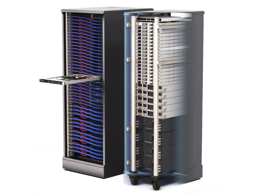
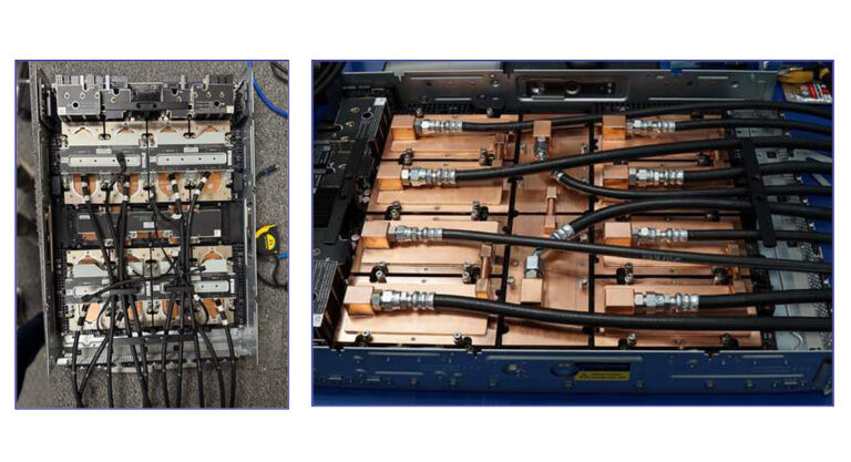
The company reports that as generative AI workloads drive larger and higher speed servers in data centers, PCB designs have become more multilayered and complex. This complexity increases the need for precise via modeling, as vias—conductive holes connecting PCB layers—directly impact signal integrity, especially at frequencies above 50 GHz. OKI Circuit Technology claims that conventional modeling approaches fail to fully represent the effects of manufacturing variations or material properties at high frequency, reducing correlation between simulation and actual outcome.
OKI Circuit Technology’s new simulation technology addresses this by using three-dimensional electromagnetic field analysis tools, along with a proprietary database built from in-house evaluation data. The process evaluates and optimizes via structure, dimensions, and manufacturing margins before fabrication, reflecting characteristics of OKI’s own manufacturing lines. According to OKI Circuit Technology, this approach enables accurate via modeling and reliable signal characteristics for high-speed, high-frequency PCB applications.
Data center applications are specifically highlighted as a key target for this technology, particularly for high-speed transmission infrastructure supporting AI workloads. OKI Circuit Technology will demonstrate the solution at SWTest Asia 2025 in Fukuoka, Japan, from November 20 to 22, 2025. More technical details and resources are available on its High-speed Transmission site.
Source: OKI