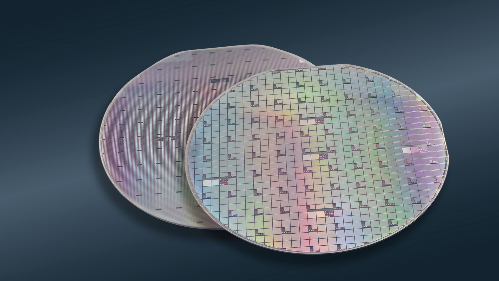
onsemi has announced the introduction of its vertical gallium nitride (vGaN) power semiconductors, which it claims set new standards for power density, efficiency, and ruggedness. These vGaN devices are built on proprietary gallium nitride-on-gallium nitride (GaN-on-GaN) technology developed and manufactured at its Syracuse, New York facility and are currently sampling in 700 volt and 1,200 volt versions to early access customers. The technology is supported by over 130 granted patents relating to process, device structure, manufacturing, and systems implementation.
According to onsemi, the vertical architecture of its vGaN devices enables current to flow vertically through the semiconductor, supporting higher operating voltages and faster switching frequencies compared to lateral GaN devices that typically use silicon or sapphire substrates. This design leads to reductions in energy loss—onsemi reports nearly 50 percent lower losses—while also providing greater thermal stability and reliability under demanding operating conditions. The ability to operate at higher frequencies enables a further reduction in system size, particularly in the sizing of passive components such as capacitors and inductors.
For data center applications, onsemi notes that vGaN devices are intended to support the power requirements of high-density racks and AI compute clusters by increasing power density and lowering the cost per rack. The company claims that these devices can significantly reduce component count and system size for 800 volt direct current to direct current (DC-DC) converters used in AI computing systems. Other stated application areas include electric vehicle traction inverters, EV charging infrastructure, renewable energy inverters, energy storage systems, industrial automation, and aerospace or defense systems.
In onsemi’s view, the monolithic vertical GaN construction enables devices that are approximately one-third the size of lateral GaN equivalents, with improved ruggedness and reliability. All vGaN wafers are processed at the Syracuse, New York fabrication facility.
Source: onsemi