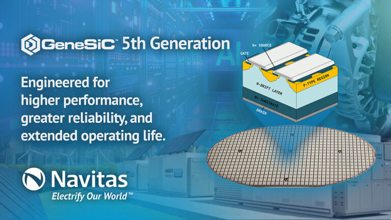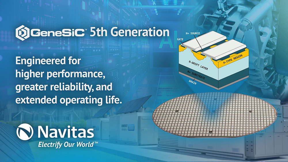
Navitas Semiconductor has announced its fifth-generation GeneSiC high-voltage silicon carbide (SiC) Trench-Assisted Planar (TAP) MOSFET technology platform, targeting an “industry leading 1200V line of MOSFETs.” Navitas positions the platform as a performance and reliability step over its prior 1,200 V generation, and as a complement to its fourth-generation ultra-high-voltage (UHV) 2,300 V and 3,300 V GeneSiC technologies for AI data centers, grid and energy infrastructure, and industrial electrification.
Navitas says the fifth-generation MOSFETs use its most compact TAP architecture to date, combining a planar gate for ruggedness with a trench structure in the source region to improve key performance figures of merit. The company also claims the architecture “elevat[es] the efficiency and life-time reliability for high-voltage power electronics.”
On switching and conduction performance, Navitas reports a “35% improved RDS,ON × QGD figure of merit (FoM), as compared to the previous generation 1200 V technology,” which it says reduces switching losses and supports cooler operation and higher switching frequency. It also reports an approximately 25% improvement in the QGD/QGS ratio, and notes a “stable high threshold voltage specification (VGS,TH ≥ 3V)” intended to improve immunity to parasitic turn-on in high-noise environments.
For dynamic behavior and EMI control, Navitas says it has optimized the RDS(ON) × EOSS characteristic and added “Soft Body-Diode” technology to “minimiz[e] electromagnetic interference (EMI) and ensur[e] smoother commutation during high-speed switching cycles.” For qualification, Navitas states this generation is “AEC-Plus grade,” which it defines as exceeding AEC-Q101 and Joint Electron Device Engineering Council (JEDEC) standards “based on Navitas test results,” and lists reliability benchmarks including extended high-temperature reverse bias (HTRB), high-temperature gate bias (HTGB), and HTGB-R stress testing; dynamic reverse bias (DRB) and dynamic gate switching (DGS); low VGS,TH shift under extended switching stress; an extrapolated gate-oxide failure time “exceeding 1 million years” at operating VGS of 18 V and 175°C; and “exceptionally low” Failure In Time (FIT) rates for improved cosmic ray resilience.
Navitas also points to supporting documentation and a product roadmap: a TAP technology white paper is available for free download from its website, and the company says it will announce additional products built on the fifth-generation platform “during the coming months.”
Source: Navitas Semiconductor