
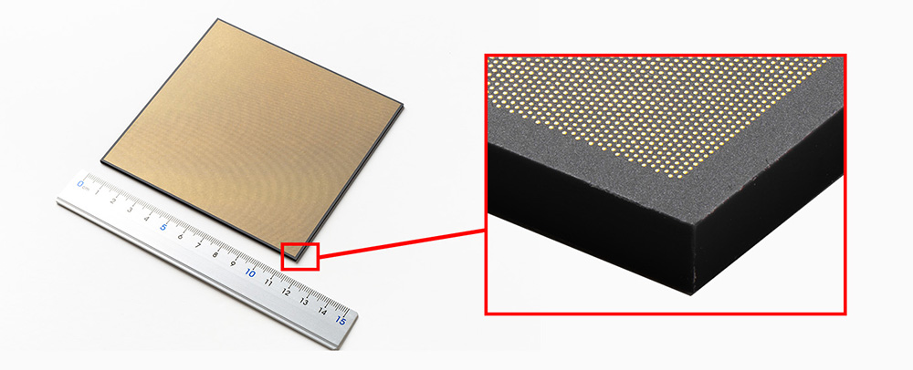
Kyocera has developed a multilayer ceramic core substrate aimed at advanced semiconductor packages used in AI data center silicon, including xPUs and switch ASICs. The company is commercializing the substrate and plans to unveil it at ECTC 2026.
Built using Kyocera’s proprietary Fine Ceramic materials, the multilayer ceramic core substrate is engineered for high-density wiring and high rigidity. Kyocera says the rigidity reduces package deformation (warpage), a persistent issue as package sizes increase and wiring density climbs in high-performance devices.
For data center engineers, the packaging angle matters because warpage and substrate stability can become practical constraints as accelerators and network silicon push into larger, denser packages, particularly in 2.5D designs. If the substrate can hold tighter mechanical tolerances while enabling finer interconnect structures, it can remove a packaging bottleneck that shows up downstream as yield, reliability, and integration limits.
What Kyocera is building
Kyocera’s substrate uses a multilayer ceramic structure intended to resist bending through assembly. The company says this can minimize warpage “during each mounting phase,” and that it can enable “slimmer substrates” while supporting further miniaturization. Kyocera attributes the slimmer-substrate point to its own simulation results (February 2026).
The company is also pointing to the way multilayer ceramic vias are formed. In its process description, vias are created while the ceramic is still pliable, prior to firing (sintering). Kyocera contrasts that with conventional organic core substrates that rely on drilling processes for via formation, and says the ceramic approach enables smaller via diameters and tighter via pitches to help with high-density, three-dimensional wiring.
Design-phase support
Alongside the physical substrate, Kyocera says it will support customer programs with simulations during the design phase, including thermal, electrical, and substrate-warpage modeling based on device performance objectives and specified mounting processes. The goal, Kyocera says, is improved customer development efficiency and meeting design objectives in the finished device.
Commercially, Kyocera is positioning the technology for advanced semiconductor packages used in AI-focused processing units (xPUs—a general term it uses for CPUs, GPUs, and other processing units) and switch ASICs, with a particular emphasis on larger, denser package substrates used in 2.5D packaging.
Source: Kyocera