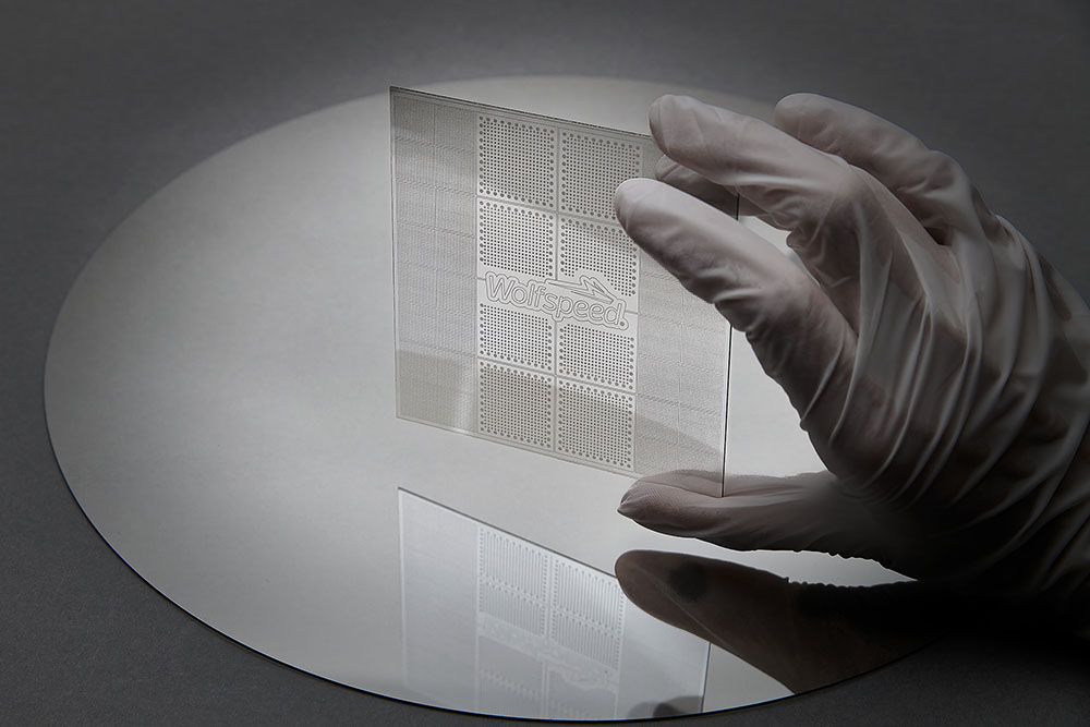
Wolfspeed says its 300 mm silicon carbide (SiC) technology platform could become a foundational materials option for advanced AI and high-performance computing (HPC) heterogeneous packaging by the end of this decade. The company is positioning 300 mm SiC substrates as a way to address thermal, mechanical, and electrical limits that it says are increasingly constraining next-generation package architectures as AI workloads push higher power density and larger package sizes.
The announcement builds on what Wolfspeed describes as a January 2026 milestone: successfully producing a single-crystal 300 mm SiC wafer. Wolfspeed said it is now engaging AI ecosystem partners to explore how 300 mm SiC substrates might help with performance barriers in advanced AI and HPC packaging.
Wolfspeed is framing the technical rationale around SiC material properties, calling out high thermal conductivity, mechanical robustness, and favorable electrical properties, and pairing that with a 300 mm format “aligned to existing 300 mm semiconductor infrastructure.” In practical terms for packaging and wafer-level processes, the company argues that a 300 mm SiC wafer format could align advanced packaging materials with leading-edge semiconductor fabrication and wafer-level packaging flows, using existing toolsets and infrastructure to support repeatable, high-volume manufacturability and cost scaling.
The company also pointed to package-size implications: Wolfspeed said a 300 mm format can enable fabrication of larger interposer and heat spreader components, which it ties to “increasingly large package form factors” and more complex multi-component assemblies for future AI systems. Wolfspeed described its work as “patent-pending innovations” intended to provide scalable “materials building blocks” for these packaging roadmaps, but did not disclose specific wafer specs beyond diameter, process details, performance targets, or product availability.
Through what it calls an “ongoing partner evaluation program,” Wolfspeed said it is collaborating with foundries, OSATs (outsourced semiconductor assembly and test providers), system architects, and research institutions to assess technical feasibility, performance benefits, reliability, and integration pathways. Wolfspeed said the goal is to accelerate learning, de-risk adoption, and prepare for hybrid silicon carbide–silicon packaging architectures it expects will be required by future AI workloads.
“As AI workloads continue to increase package size, power density, and integration complexity, we believe new materials foundations will be increasingly important to extend advanced packaging roadmaps,” said Elif Balkas, Chief Technology Officer at Wolfspeed. “Our 300 mm silicon carbide platform is designed to align SiC’s material advantages with industry-standard manufacturing infrastructure and expand the solution space for next-generation AI and HPC packaging architectures.”
Wolfspeed did not provide pricing, a commercialization timeline beyond “by the end of this decade,” or specific partner names in the announcement.
Source: Wolfspeed