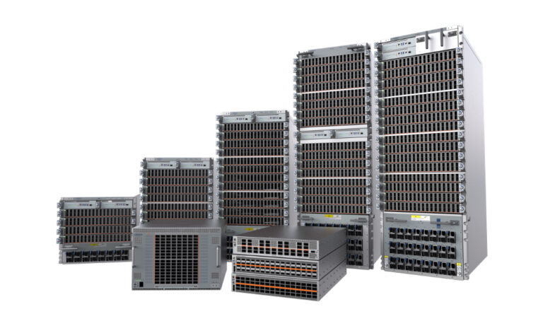
OKI is launching a set of electronics manufacturing services (EMS) aimed at AI server equipment makers, covering everything from PCB design and fabrication through assembly, test, and rework. The company puts a specific emphasis on building and servicing large-size multi-layer printed circuit boards (PCBs) intended for densely mounted AI semiconductors.
OKI says the EMS scope spans design and production of large-size multi-layer PCBs that incorporate its proprietary high heat dissipation technology and support high-speed, high-capacity data transmission, plus component procurement, PCB component mounting, system assembly, testing, and reworking. The launch date is March 25, 2026, with pricing quoted individually, and a sales target of JPY 1 billion in FY2026.
For data center engineers, this is one step removed from the facility itself, but it matters because packaging, board-level thermals, and manufacturability shape what ultimately shows up in racks. High-density AI boards are expensive to scrap, and long lead times for complex components can turn a single assembly defect into schedule risk that ripples into deployment timelines.
OKI points to production challenges it’s targeting, including placement accuracy, managing warping and interference caused by thermal expansion differences between PCBs and components during high-temperature heating, countermeasures for operational heat from densely mounted AI semiconductors, and finding solder defects in contact points that can’t be identified by AOI (Automated Optical Inspection). The company also calls out expanded traceability requirements, a growing number of inspection items, and the increasing difficulty of rework once large, costly AI semiconductors have been mounted.
On the PCB side, OKI says it will use simulation and manufacturing technologies for multi-layer PCBs that incorporate its proprietary PCB heat-dissipation approach using an embedded copper coin. For inspection and test, the company highlights high-speed X-ray solder inspection and automation technology for functional testing, alongside high-mix low-volume production capabilities it says are aimed at high-quality, high-reliability output.
Rework is a central part of the pitch: OKI says its reworking line combines proprietary jigs with handwork by skilled technicians and advanced soldering techniques to deliver short-lead-time reworking, including for AI semiconductors with over 10,000 pins.
Comprehensive EMS and the company’s PCB heat dissipation technology pages include additional program details.
Source: OKI