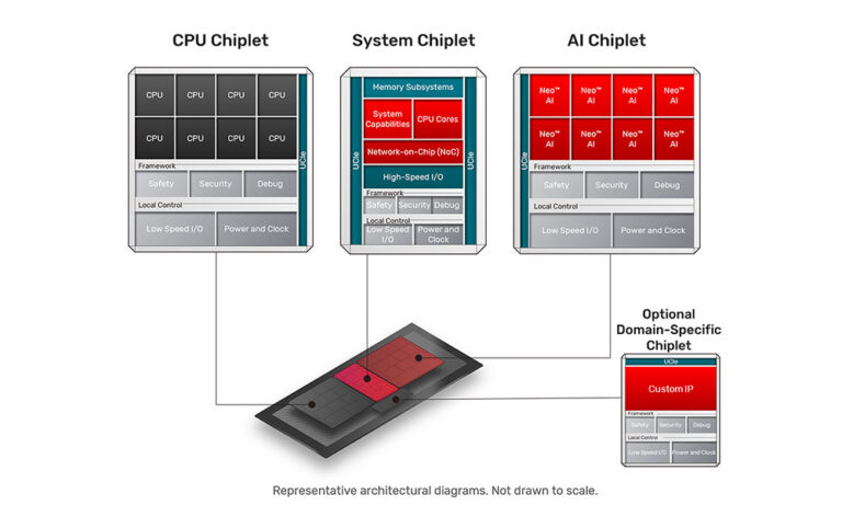
The Open Compute Project Foundation (OCP) has announced the release of a Universal Die-to-Die (D2D) Transaction and Link-Layer specification designed to promote silicon diversity in high-performance AI and high-performance computing (HPC) clusters. The new specification includes support for Universal Chiplet Interconnect Express and targets the development of reconfigurable AI clusters optimized for specialized workloads, according to OCP.
OCP reports that the universal link layer defines customizable profiles to map upper-level transaction layer services to the underlying physical layer (PHY) via the link layer. This enables designers to select a PHY without affecting other layers, facilitating greater flexibility in silicon integration. The specification uniquely combines multiple physical layer bindings with low-latency, low-overhead packetization for protocol traffic between chiplets, allowing efficient data exchange and extensibility for different design protocols.
The universal link layer supports key features: extensibility for interface profiles that enable native bus protocols to be packetized and transported for chiplet interoperability, portability across different die implementation methodologies and process nodes, and scalability with multiple PHY slices at various data rates. These attributes make the new specification relevant for a range of system-in-package designs in data center AI and HPC cluster deployments, as well as in other sectors like automotive.
Cliff Grossner, Ph.D., Chief Innovation Officer at OCP, said, “The OCP recognized several years ago that innovation in silicon needed to be amplified, just as the constraints of larger silicon dies were beginning to impede progress. Through its Open Chiplet Economy Project, the OCP has established a strong community to deliver on the new standardizations, tools and best practices around technical and business workflows that are required for a truly open economy, where vendors sell chiplets embodying their IP to integrators that then build specialized System in Packages (SiPs).”
Balaji Baktha, Founder and CEO at Ventana Micro Systems, commented, “Ventana has been at the forefront of the chiplet revolution, driving adoption of open, scalable solutions across the industry. Ventana is proud to continue its contributions within the OCP Community, enabling high-performance systems across Data Center, AI, and Automotive markets. What makes this specification unique is its efficiency and its ability to work with existing protocols and fabrics. This means chiplet-based designs can achieve near-monolithic performance without costly protocol bridges or complex conversions, accelerating innovation while keeping integration simple and open.”
OCP has also announced the Chiplet Marketplace, which went live in October 2024, offering a catalog of standalone chiplets, design and manufacturing services, chiplet-aware electronic design automation tools, and reference materials for system-in-package designers and builders.
Anu Ramamurthy and Jawad Nasrullah, Open Chiplet Economy Project leads at OCP, stated, “We are at an inflection point where chiplet vendors have a fairly complete set of standards and tools available to build chiplet product sets. The market leaders developing chiplets are still playing a very important role filling gaps that they identify in current standards, and we expect to see these additional learnings materialize as updates to existing standards as the Open Chiplet Economy matures.”
Source: Open Compute Project Foundation