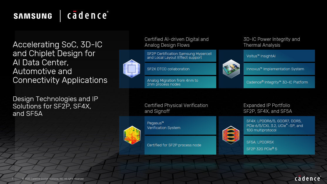
Cadence Design Systems has expanded its collaboration with Samsung Foundry through a new multi-year agreement for memory and interface intellectual property (IP) development, specifically targeting AI data center, high-performance computing (HPC), and automotive markets. This agreement encompasses Samsung’s advanced SF4X, SF5A, and SF2P process nodes and is built upon joint AI-driven design methodologies.
The Cadence digital full flow has achieved certification for Samsung’s latest SF2P process node, incorporating technologies such as Samsung’s Hyper Cell methodology and Local Layout Effect (LLE) timing accuracy enhancement. Cadence’s Pegasus Verification System is also certified for SF2P, enhancing scalability and performance in physical verification to meet signoff accuracy and runtime efficiency goals.
“Cadence’s suite of digital tools from RTL to GDS is now certified for Samsung’s latest SF2P process node, supporting advancements like Hyper Cell and LLE 2.0 technologies,” said Hyung-Ock Kim, vice president and head of the Foundry Design Technology Team at Samsung Electronics. “Cadence and Samsung are also collaborating closely to enable analog migration, enhance power integrity and improve thermal and warpage analyses for 3D-ICs using GPU acceleration.”
The partnership includes co-development successes like automated analog design migration from 4nm IP to a 2nm node, significantly reducing design turnaround time while preserving design intent. Additionally, the collaboration demonstrated a comprehensive Front-End Module and Antenna-in-Package co-design flow specifically tailored for next-generation mmWave applications based on Samsung’s 14nm FinFET process, significantly streamlining development stages.
Cadence and Samsung have collaborated on comprehensive full-flow power integrity analysis for 3D-IC designs. On Samsung’s SF2 node, Cadence’s Voltus InsightAI tool successfully resolved 80-90% of IR-drop violations on a high-speed CPU chip with minimal timing and power impacts.
Source: Cadence Design Systems