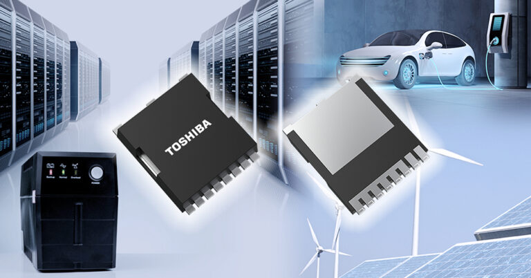
Toshiba Electronic Devices and Storage Corporation has signed a memorandum of understanding (MOU) with SICC, a China-based developer of silicon carbide (SiC) wafers, to explore technical collaboration aimed at improving the characteristics and quality of SiC power semiconductor wafers. Under the agreement, Toshiba and SICC will discuss joint efforts to enhance wafer quality and reliability and expand SICC’s supply of high-quality SiC wafers to Toshiba.
SiC power semiconductors are critical for efficient power conversion and control, especially in demanding high-temperature settings like electric vehicles and renewable energy systems. According to details from Toshiba, ensuring wafer reliability and stable quality remains challenging as the industry pushes for further efficiency improvements in power electronics.
Toshiba reports an established background in developing and producing SiC power semiconductors for railway systems and is expanding development for automotive and power supply applications. The company targets reductions in power losses and improvements in reliability across future high-efficiency power conversion platforms. Achieving these improvements requires advanced SiC wafer technology and stable supply, which it intends to address through this collaboration with SICC.
SICC, which began operations in 2010 and went public in China in 2022, focuses exclusively on single-crystal SiC wafer development and manufacturing. The company claims a top-five global position in related intellectual property and, in 2024, introduced the industry’s first 12-inch SiC wafer. In 2025, SICC announced the release of 12-inch wafers across all product types, including n-type, semi-insulating, and p-type substrates. SICC’s stated aim for this technical partnership is to align SiC wafer technology with semiconductor manufacturers’ requirements, improving both quality and reliability.
Toshiba and SICC have indicated they will continue discussions to determine the specific scope and mechanisms of collaboration under the MOU.