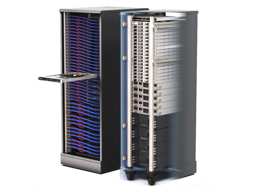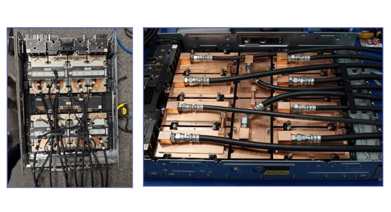
Sarcina has launched its UCIe-A/S Packaging IP, a package-level die-to-die (D2D) interconnect aimed at chiplet-based architectures used in HPC, AI, data center infrastructure, next-generation networking platforms, and co-packaged optics. The company is pitching the IP as a way to deliver UCIe connectivity in-package, over an interposer or substrate, without teams having to build complex packaging solutions in-house.
Sarcina frames the offering as packaging-focused interface IP rather than traditional silicon-based interface IP, targeting the physical D2D interconnection layer within the package. The company lists signal integrity (SI), power integrity (PI), routing efficiency, silicon utilization, and manufacturability as key design dimensions the IP is meant to address.
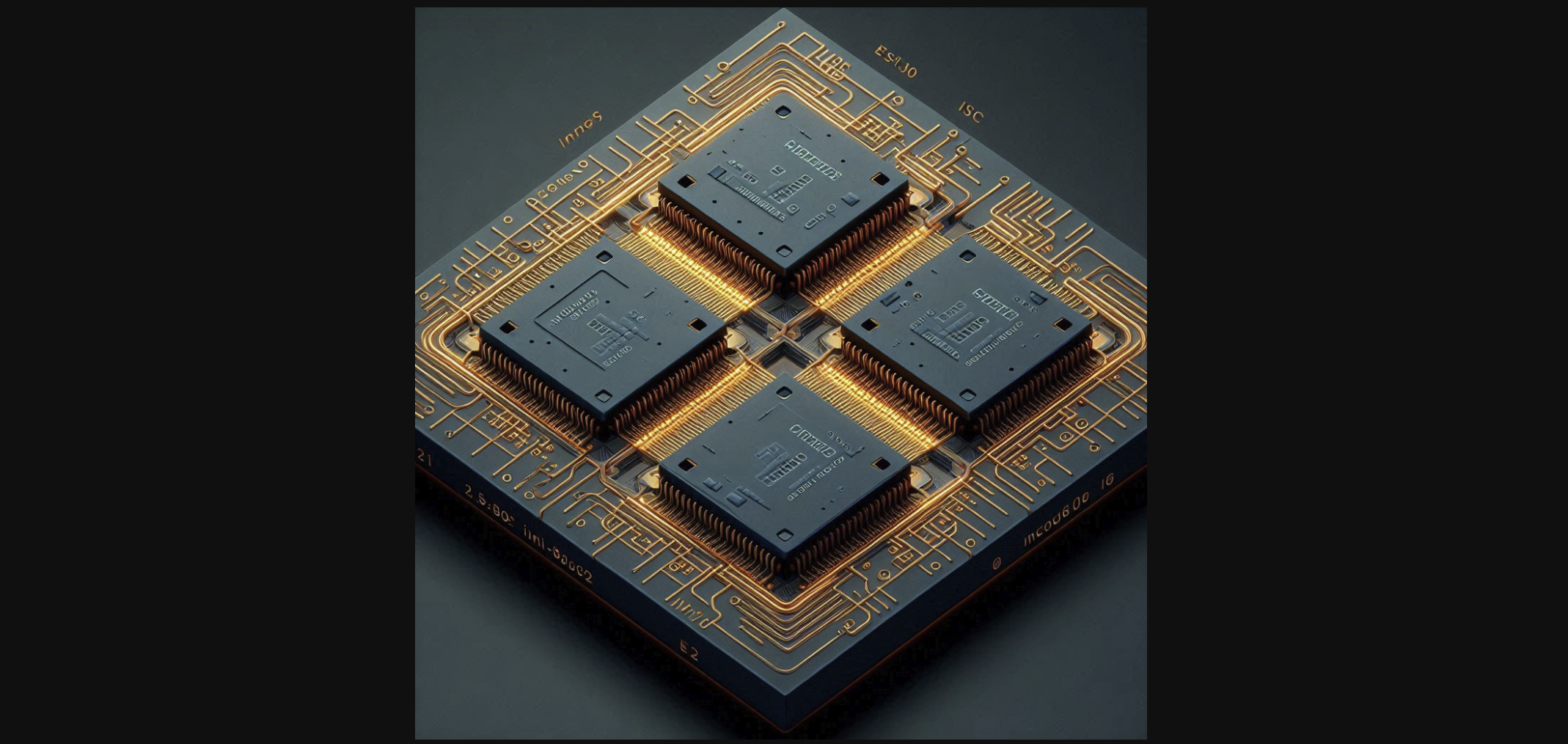
The UCIe-A Packaging IP is designed to use a minimal number of copper redistribution layers (RDL) while supporting a 64-bit D2D interconnect using a standard UCIe-A module. Sarcina says the architecture aligns interconnect width with the die bump “beachfront,” allowing multiple modules to be placed along the die edge without increasing module-to-module spacing, which it says can reduce die area overhead and system cost.
On standards and signaling, Sarcina states the UCIe-A Packaging IP is fully compliant with UCIe 2.0 and supports data rates up to 32 GT/s. The company also points to channel simulations showing “strong eye margin performance.”
The UCIe-S Packaging IP is described as a scalable, modular approach: it starts with a 16-bit configuration, then doubles bandwidth to 32 bits by stacking modules behind the primary interface without increasing beachfront width. Sarcina says the same method can scale to 64, 128, 256 bits, and beyond along the die edge.
At the package level, Sarcina says UCIe-S confines routing within the D2D region to allow tighter module placement while minimizing substrate resource consumption, freeing routing area for functions such as power delivery. The company cites simulation results with extrapolated eye contours outside the mask at a BER of 1E-15 at full 32 GT/s data rates, and says the technology is undergoing silicon qualification.
For data center and AI infrastructure engineers, the practical angle is straightforward: if you’re betting on chiplets to build larger systems (and to keep I/O and memory bandwidth scaling), the packaging interconnect quickly becomes the schedule and risk driver. Packaging IP that’s already aligned to UCIe 2.0 and designed around die-edge “beachfront” constraints could reduce iteration cycles, but the real test will be how it behaves through qualification and production ramps.
“We’re empowering our customers to leverage UCIe connectivity at the package level—reducing complexity while accelerating time-to-market,” said Eric Gunn, VP of Sales at Sarcina. Sarcina says flexible licensing options are available, and that the IP is offered as part of its advanced packaging design and production services.
Source: Sarcina