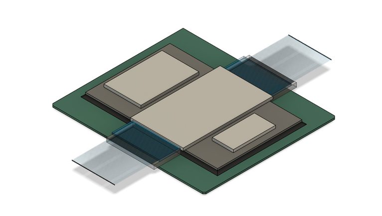

Alpha and Omega Semiconductor has introduced the AOPL66801, an 80 V MOSFET half-bridge that packages two vertically stacked MOSFET dies into a DFN 6 x 5 AmpStack package. The approach targets higher power density in power conversion designs by putting the high-side and low-side devices into a single package footprint, rather than placing two discrete DFN 5 x 6 MOSFETs on the PCB.
The AOPL66801 uses stacked-die construction with the two MOSFETs connected as a half-bridge. Alpha and Omega Semiconductor also uses an optimized clip design at the switch node (the connection between the two MOSFETs) to reduce parasitic inductance between the high-side and low-side devices. Lower inductance at the phase node is intended to reduce voltage ringing and the associated electrical stress on the MOSFETs compared with a standard discrete layout.
Layout-driven parasitics are often the hidden limiter in fast-switching power stages. Packing a half-bridge into one package can simplify current loops and make repeatable performance easier to achieve across PCB revisions, but it also concentrates thermal and switching stress into a tighter footprint, which puts more pressure on board-level heat spreading and airflow or cold-plate design.
The package includes a Kelvin sense pin intended to maintain gate-voltage stability during large di/dt switching and to provide a more effective drive path for the high-side device, reducing losses. Alpha and Omega Semiconductor lists a maximum junction temperature of 175 °C for the part.
Alpha and Omega Semiconductor’s Peter H. Wilson, senior director of the MOSFET product line, said, “Our new AmpStack™ half-bridge packaging is a game-changer for designers looking to increase power density compared to solutions using two DFN 5×6 packages,” adding, “by designing the package for low source parasitic inductance, we’ve drastically reduced phase node ringing and MOSFET stress.”
Key specs (AOPL66801)
Alpha and Omega Semiconductor lists the AOPL66801 in a DFN 6 x 5 package with 80 V VDS and ±20 V VGS for both the high-side (Q1) and low-side (Q2) MOSFETs. Maximum RDS(ON) is 2.2 mΩ at VGS = 10 V for both devices. Rated ID is 304 A (high side) and 215 A (low side). Capacitances are listed as Ciss 4900 pF, Coss 1400 pF, and Crss 34 pF, with total gate charge Qg of 70 nC.
Pricing and availability
The AOPL66801 is available in production quantities with a 16-week lead time. Pricing is listed at $6.16 per unit in 1,000-piece quantities.
Source: Alpha and Omega Semiconductor