
Advanced Semiconductor Engineering (ASE) has announced the launch of IDE 2.0, a major upgrade to its Integrated Design Ecosystem platform. IDE 2.0 incorporates artificial intelligence (AI) to accelerate package design iterations and optimize chip-package interaction analysis. ASE claims this platform reduces time-to-market for complex artificial intelligence (AI) and high-performance computing (HPC) applications.
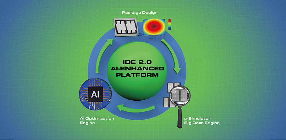
IDE 2.0 offers a cloud-based e-Simulator that employs AI engines for predictive chip-package interaction risk assessments, as well as integrated analysis and optimization of design, data, and manufacturing inputs. According to ASE, IDE 2.0 improves efficiency in advanced packaging design and streamlines workflows.
The new platform introduces an AI-driven feedback framework that continuously synchronizes design and simulation in real time. This capability assists in managing architectural complexities for multi-die, chiplet, and heterogeneous integration designs. IDE 2.0 combines multiphysics-based simulation, data correlation, and AI-powered insights to accelerate and improve design precision, reliability, and risk prediction.
ASE reports that IDE 2.0 can shorten the design-analysis cycle from weeks to hours. Key technical enhancements include simulation acceleration—reducing design iteration time by more than 90%, integrated multiphysics simulations that cover electrical, thermal, mechanical warpage, and reliability domains, and AI-based risk prediction that produces rapid risk assessments within 60 seconds.
“By integrating characterized material and simulation databases with AI-driven capabilities, IDE 2.0 delivers precise insights into chip-package interaction and residual stress,” said Dr. C.P. Hung, Vice President of Corporate Research and Development, ASE. “Customers can rapidly model, customize, and optimize designs – reducing prototypes, costs, and time-to-market while protecting IP. It’s a major leap forward for packaging architects innovating in the AI era.”
IDE 2.0 is available now as part of ASE’s VIPack advanced packaging platform for collaborative design with ASE customers. ASE specifically highlights its relevance for data center, AI, and HPC applications, while also supporting broader markets.