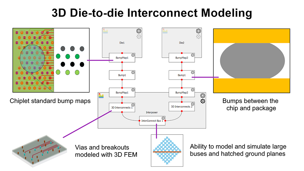
Keysight has introduced 3D Interconnect Designer, a new Electronic Design Automation (EDA) tool aimed at designing and optimizing three-dimensional (3D) interconnects for high-chiplet and three-dimensional integrated circuit (3DIC) advanced packages used in AI infrastructure and data center applications. Keysight says the tool targets the growing complexity of multi-die and stacked-die interconnect design, where traditional workflows can become inefficient and drive additional design spins and longer development cycles.
Keysight positions the tool as a dedicated workflow for 3D interconnect design and optimization, covering structures such as vias, transmission lines, solder balls, and micro-bumps, with a focus on maintaining signal and power integrity in dense systems. It also supports complex geometries such as hatched or waffled ground planes, which Keysight says can be critical for addressing manufacturing and fabrication constraints in advanced packaging, including silicon processes such as interposers and bridges.
Keysight reports three primary benefits: faster design cycles through automation that reduces manual steps; lower compliance risk by validating designs early against emerging standards including Universal Chiplet Interconnect Express (UCIe) and Bunch of Wires (BoW), as well as ex VTF (Voltage Transfer Function); and more accurate performance prediction using electromagnetic-based simulation for electrical analysis of printed circuit board (PCB) and package 3D interconnect designs.
The company says 3D Interconnect Designer integrates with Keysight’s EDA tools and is also available as a standalone version, allowing teams to add 3D interconnect optimization to existing workflows. Keysight also notes that when used with Chiplet PHY Designer, engineers can design and optimize 3D interconnects specifically for chiplets and 3DICs to reduce costly iterations in multi-die systems.
“With today’s complexity, manual 3D interconnect design and optimization have become a significant bottleneck,” said Nilesh Kamdar, EDA Design and Verification General Manager at Keysight. “By streamlining the process and providing early insights into potential issues like signal and power integrity, we’re enabling engineers to get products to market faster and deliver compliant designs on tighter timelines.”
Source: Keysight