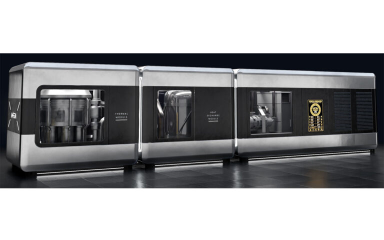
MemryX has announced the roadmap for its next-generation MX4 accelerator, designed to bring its “at-memory” dataflow architecture from edge devices into the data center. The MX4 uses 3D hybrid-bonded memory to address bottlenecks known as the “memory wall,” an issue where memory bandwidth, capacity, and efficiency limit AI inference workloads more than pure compute power.
Currently, MemryX reports that its MX3 silicon is in production, delivering greater than 20× better performance per watt than mainstream graphics processing units (GPUs) for specific AI inference tasks. Building on this, the MX4 introduces a dedicated direct-to-tile memory interface using ~5 micron (µm)-class hybrid bonding, aiming to validate this integration in a 2026 test chip program conducted with an undisclosed 3D memory partner.
The MX4 targets data center workloads that outgrow current 2.5D high-bandwidth memory (HBM)-based architectures, especially for large action models (LAMs), high-resolution multimodal vision, and real-time recommendation engines. It physically bonds high-bandwidth memory directly to compute tiles, reducing data movement and focusing on high-efficiency computation.
On a technical level, the MX4 departs from traditional synchronous chip designs by continuing MemryX’s data-driven producer/consumer flow-control model. It eliminates the need for a global clock or centralized memory controller, allowing compute tiles to operate independently based on data availability and need. This asynchronous design is paired with a distributed vertical interconnect achieved via hybrid bonding, enabling each compute engine to access memory directly. The architecture also supports a variety of 3D memory formats, including current stacked dynamic random-access memory (DRAM) and emerging ferroelectric random-access memory (FeRAM) technologies.
The MX4 will maintain software compatibility by leveraging the existing MX3 compiler and runtime tools, streamlining adoption for both existing and new users. The roadmap outlines a 2026 test chip, first customer sampling in 2027, and production scaling—eventually supporting memory configurations greater than 1 terabyte—in 2028.
“The industry has recognized that deterministic dataflow is a compelling path forward for AI inference, but both efficiency and scale are critical,” said Keith Kressin, CEO of MemryX. “By combining our production-proven architecture—including an asynchronous flow model—with 3D hybrid bonding, we are removing the physical barriers to power-efficient trillion-parameter scalability. We aren’t just building a faster chip; we are building a more practical roadmap for the future of AI.”
For more details on the MX3 architecture, visit MemryX’s technical overview.
Source: MemryX