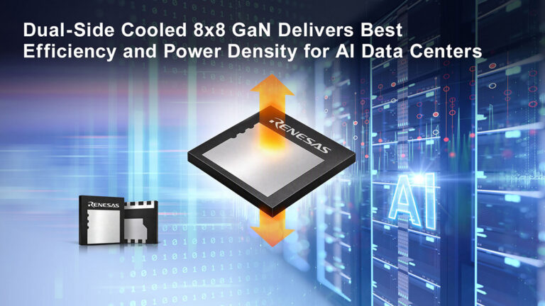

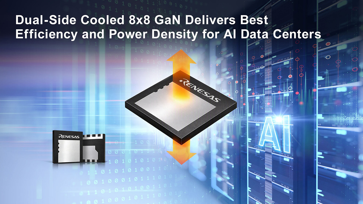
Renesas has introduced the TP65H020G4PLSGBD, a 650 V GaN device in an 8 x 8 mm dual-side-cooled (DSC) PQFN package aimed at high-density power conversion for 800 V high-voltage DC (HVDC) AI data center architectures. The part targets space- and thermally constrained power stages in megawatt-scale racks, where intermediate bus converters and sidecar power shelves are getting harder to fit and harder to cool as power rises.
The TP65H020G4PLSGBD is a D-mode device built on Renesas’ Gen IV Plus GaN architecture. Renesas lists 20 mΩ on-resistance for the device, and frames that as “one of the lowest” in the 650 V class. The company is sampling the part to major AI data center OEMs and ODMs.
Renesas is aiming the device at 800 V DC/DC intermediate bus converter (IBC) stages that step down to 48 V, 12 V, or 6 V, as well as battery backup (BBU) and capacitor bank (CBU) stages in sidecar power racks. The company also references up to 700 V operation in next-generation AI data center designs, tying the device to higher-voltage distribution schemes used to reduce current (and copper) in high-power racks.
Packaging is the headline engineering change. Renesas says the dual-side cooling approach dissipates heat from both the top and bottom of the package, and that it lowers top-side thermal impedance by 10% versus conventional top-side-cooled packages. The 8 x 8 mm PQFN footprint is also listed as 57% smaller than a 10 x 15 mm TOLT package, a meaningful board-space reduction in crowded power stages where magnetics, capacitors, and isolation spacing already fight for area.
On the drive side, Renesas says the device has low gate charge and output capacitance, includes a built-in freewheeling diode with minimal reverse recovery, and uses a high threshold voltage that runs without a negative gate bias. Practically, that “no negative bias” point matters because it can reduce gate-drive complexity compared with approaches that require special handling to keep the device off under fast dV/dt. Renesas also says engineers can drive it with a standard silicon gate driver and switch into the MHz range to reduce passive component size and BOM cost.
Renesas also points to a validated reference platform: a 6 kW, 800 V-to-48 V LLC DC transformer (DCX) reference design using the new device and controlled by a Renesas RA6T3 MCU. Renesas reports 2.6 kW/in³ power density, and says per-module testing measured full-load efficiency 0.21% higher than an equivalent TOLT-based board. The company also cites 800 V-to-12 V and 6 V DC/DC IBC reference designs built on the same DSC 8×8 platform.
“Customers building megawatt-scale AI data centers are running out of board space and thermal headroom before they hit their power limits,” said John Wiggenhorn, senior product line director of high-voltage GaN at Renesas. “With the industry’s first dual-side-cooled 650V GaN, we cool the device from both sides and cut the footprint significantly, so designers can move more power through the intermediate bus without redrawing the board or adding more cooling hardware.”
The TP65H020G4PLSGBD is sampling now, and Renesas says mass production is planned for mid-2027.
Source: Renesas