
Atomica has launched its AI Photonic Integration Platform, a microfabrication platform aimed at one of the harder problems in AI infrastructure hardware: integrating photonics with electronics, memory, thermal structures, and package-level interfaces in a way that’s actually manufacturable at scale.
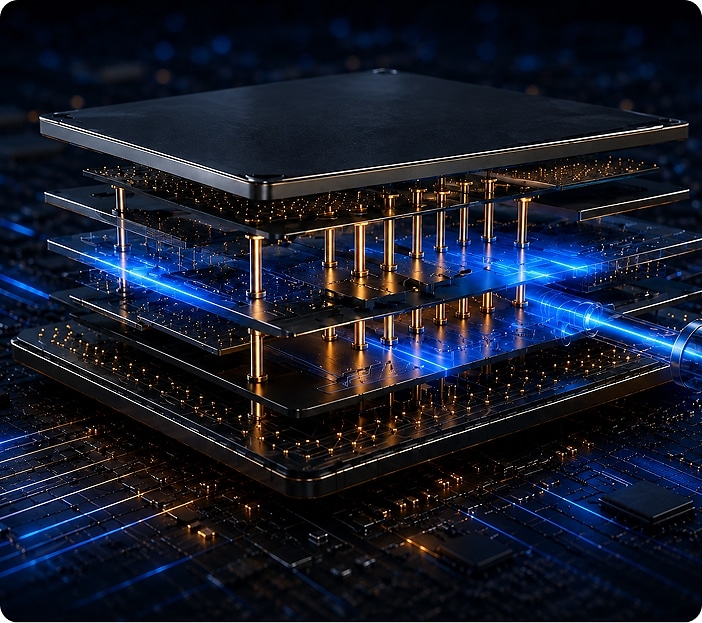
The AI Photonic Integration Platform is built around a “configurable microfabrication pathway” that spans interposers and vias, bonding, optical alignment, and wafer-level packaging. Atomica describes it as a platform for customers developing photonic and heterogeneous AI hardware where optical functions have to live alongside dense electrical I/O and aggressive thermal constraints in compact packages.
On the process side, Atomica lists support for silicon and glass interposers, through-silicon vias and through-glass vias, redistribution layers, wafer-level packaging, bonding, cavities, optical alignment structures, and customer-specific process layers. The company’s pitch is integration: photonic, electronic, memory, and thermal components may be built on different substrates and materials, with different alignment, stress, thermal, and reliability requirements, and the job is to bring them together without sacrificing electrical performance, optical performance, or manufacturability.
For data center engineers, the practical takeaway is that packaging and interconnect are increasingly gating factors for AI systems, not just compute. Bandwidth, interconnect density, signal integrity, thermal management, optical alignment, and package-level integration show up as system constraints long before a cluster hits the theoretical limits of its processors.
“The next leaps in AI hardware will not come from any single chip,” said Eldon Klaassen, CEO of Atomica. “They will come from integration—bringing logic, memory, optics, and thermal management together into a manufacturable system.” He also said, “The challenge is no longer simply whether individual devices perform. The challenge is whether optics, electronics, memory, and thermal structures can be integrated with the precision and repeatability required for scalable manufacturing.”
Atomica positions the platform as the third in its series of AI infrastructure platforms, following its AI Optical Connectivity Platform and AI Optical Source Platform. The company says the three are intended to cover complementary parts of the AI optical hardware stack, with the new integration platform tying optical functions into the broader substrate and packaging structures.
Atomica lists target applications including AI accelerators, high-bandwidth memory integration, chiplet packages, data-center switches, optical I/O modules, co-packaged and near-packaged optics, photonic integrated circuit packaging, optical engines, and external laser-source packages. A company eBook is available on the platform page at atomica.com/ai-photonic-integration-platform/.
Source: Atomica