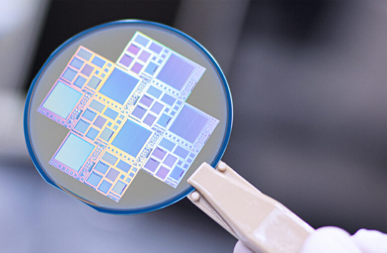
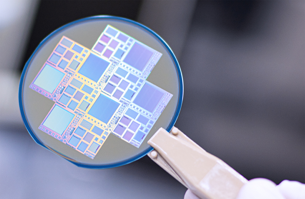
Great Sky and a group of US fusion research organizations have developed and tested a superconducting neural-network chip aimed at real-time fusion plasma monitoring and control. The work involved Brookhaven National Lab, Princeton Plasma Physics Laboratory, and the DIII-D National Fusion Facility, and it focused on running AI tasks fast enough to ingest high-rate tokamak signals without falling behind.
The chip is based on what Great Sky calls a superconducting optoelectronic network (SOEN). Instead of using silicon transistors like conventional CPUs and GPUs, the device implements analog neural networks using superconducting circuitry with optical communication.
In demonstrations described by the team, the latest chip performed three tasks tied to tokamak operations. Two tasks used data collected at the DIII-D tokamak for anomaly classification and disruption prediction. That data was sampled at 1 million samples per second, and the team reported the chip “had no problem keeping up” with that rate.
A third task used simulated data from TORAX, a tokamak simulator developed by the Google DeepMind Fusion team. In that test, the chip processed simulated signals to predict sawtooth instabilities, which are critical events in tokamak operation. The group described this as a step toward using the chips as part of real-time plasma state simulation used for tokamak control and stabilization.
For data center engineers watching AI hardware alternatives, the interesting technical bet here isn’t just “faster AI”—it’s the idea that analog neural networks built with superconducting circuitry and optical links can target extreme low-latency inference loops. But superconducting hardware carries practical integration constraints, including cryogenic operation, that will matter at least as much as any raw throughput claims when it comes to deployments outside specialized environments.
“It’s incredible to see the team processing data from our tokamak,” said Richard Buttery, Director of DIII-D. “The folks here at DIII-D are very excited to see how this chip can impact diagnostics and control for the fusion industry.”
Great Sky says it has been developing the technology for over a decade, starting at the National Institute of Standards and Technology before spinning out into the current company. “This is our largest chip to date, and it’s great to see it processing high-speed data directly measured from a tokamak,” said Jeff Shainline, founder and CEO of Great Sky. He added that the team plans to demonstrate a next-generation chip with a “10x larger neural network” in December.
Great Sky has not provided pricing or commercial availability details for the chip in the information shared.
Source: Great Sky